The infrastructure for designing hardware hasn't changed in decades. People study electrical engineering, watch software engineers ship with AI copilots and instant feedback loops, and choose software instead. AI got dramatically better. The tooling didn't. Everyone in the industry is hitting the same wall -- robotics teams, defense contractors, two-person startups. The tools don't solve the hard problem. We took a different approach. Instead of trying to get AI to click through a GUI or use visual understanding of what's on screen, we built our own low-level representation of the design problem. The AI reads and writes the structure directly -- components, connections, constraints, spatial relationships -- and the visual feedback loop is the last check, not the first. It works. It's the best thing in this category right now, and it's not close. And the models are only going to keep getting better.
The Pain
A friend of mine went to the doctor for TMJ. The doctor told him to massage his jaw with warm water from a cup. That was the treatment. It worked, but only at home. He couldn't carry a cup of water around with him, so outside the house, the pain just came back.
So he decided to build his own device. A small handheld wand to treat it himself. Simple circuit board, basic firmware, nothing crazy. Vibrations and heat to mimic the warm water treatment, just portable. He wrote the firmware with AI in a weekend. The software wasn't the hard part anymore. The PCB design took him seven months. Yes, seven months of back-and-forth for a board that fits in a wand.
And there are thousands of people like him. Engineers, robotics teams, medical device founders, small hardware companies - all hitting the same wall the moment they need a circuit board designed.
What's Still Manual
The parts that are still extremely manual, even for experienced engineers: component selection, schematic generation, iteration loops. The stuff you do over and over before you even get to layout. We're working with hardware teams and engineers all over the U.S. and China who are iterating quickly, and they feel this pain the most.
Take footprint creation. Every time an engineer uses a new component, they have to build a footprint for it from scratch: open the datasheet, find the mechanical drawing, measure every pad dimension, translate that into their EDA tool, verify it, test it. Fifteen minutes minimum, for a single part. And they do this over and over - every new component, every project, every engineer on the team. It's not engineering. It's information retrieval disguised as engineering. Pure overhead that adds up to days across a project, and every hardware team on earth is doing the exact same work in parallel.
Here's what that looks like in Trace:
Beyond Design
Longer term, this naturally expands into component sourcing and manufacturing workflows - because we sit at the exact point where those decisions get made.
The $19 Billion Problem
If you ask an electrical engineer why their workflow is so manual, they'll tell you that's just how it is. That's the answer. Not because they like it, because nothing better exists. The EDA industry has operated this way for decades. Electronic design automation is a $19 billion industry that underpins everything from consumer electronics to aerospace and defense systems. The tools haven't meaningfully changed, and the problem itself is brutally hard.
Why It's Hard
And when I say hard, I mean it. PCB design is a combinatorial optimization problem. The same class as the traveling salesman problem, but worse. Even a simple board with 50 components and 10,000 possible grid positions has more placement combinations than there are atoms in the universe. And that's just placement.
Experienced PCB designers will tell you the same thing: routing isn't the hard part. If placement is right, routing mostly follows. The real challenge is deciding where everything should go in the first place.
On top of that combinatorial search space sits the physics: electromagnetic fields that move in time, behavior that changes with frequency and temperature, materials that are imperfect and nonlinear, fields that couple and interact with each other. Add manufacturing variance, current densities, thermals, signal integrity.
And if any of it isn't carefully accounted for, the board either doesn't work or literally self-destructs. It has to be 100%, not 90% correct.
There's no polynomial-time solution. You can't brute-force it. The best algorithms are heuristics. Educated guesses built on decades of human intuition, and that's exactly why the tools have stayed the way they are. The industry has hit a local maximum. You can't optimize a manual workflow into an automated one. You need a fundamentally different approach. The way hardware gets designed is about to change.
Tool Lock-In
This is also why engineers are so conservative about their tools. When your design has to be 100% correct, you don't switch to a new tool version just because it has a nicer UI. You stick with what you know works. Some engineers won't even upgrade from one version of Altium to the next because their entire workflow is built around the specific behavior of the version they're on. A bug in the new version could mean a failed board. That kind of environment doesn't reward experimentation. It rewards muscle memory. And it's part of why the industry has been so slow to change.
There are millions of PCB designers and engineers working globally. The EDA market they depend on is worth over $19 billion and growing fast, projected to hit $31 billion by 2030. But EDA software is just the design layer. Every design decision (which components to use, which manufacturer to send the board to, which supply chain to depend on) flows downstream into a global electronics components market worth nearly half a trillion dollars. Whoever controls how engineers make those decisions controls where that spend goes.
The Aging Workforce
Here's the problem though: until recently, the largest segment of PCB designers was over 50 years old. More than half the workforce is in the back half of their careers. And the pipeline behind them is nearly empty.
This isn't a small gap. By 2033, the U.S. manufacturing sector will need 3.8 million new workers, and nearly half those jobs are projected to go unfilled. The semiconductor industry needs over a million additional skilled workers globally by 2030. And the people who know how to design it are aging out. The demand for hardware is exploding. AI chips, IoT, EVs, defense, and space.

The Robotics Boom
Robotics alone saw $14 billion in startup funding in 2025, nearly double the year before. Figure AI raised over $1 billion at a $39 billion valuation to build humanoid robots. Skild AI tripled to $14 billion. Apptronik raised $520 million with Google, Mercedes-Benz, and John Deere backing them. Every one of these companies needs custom motor controllers, sensor arrays, power boards, and compute modules. All custom PCBs. The engineers to design them don't exist yet.

The Knowledge Problem
Most of what makes a great PCB designer great was never written down. It was learned on the job, over years, through mentorship and mistakes. There's no university program that teaches you how to do real PCB layout. There's no bootcamp. IPC is trying with apprenticeship programs, but they can't scale fast enough.
So the knowledge stays locked up. Experienced engineers hoard it not out of selfishness, but because there's no good way to transfer it. The feedback loop between the people who know and the people who want to learn is so broken that young engineers just give up. They look at the tooling, look at the learning curve, and choose software instead.
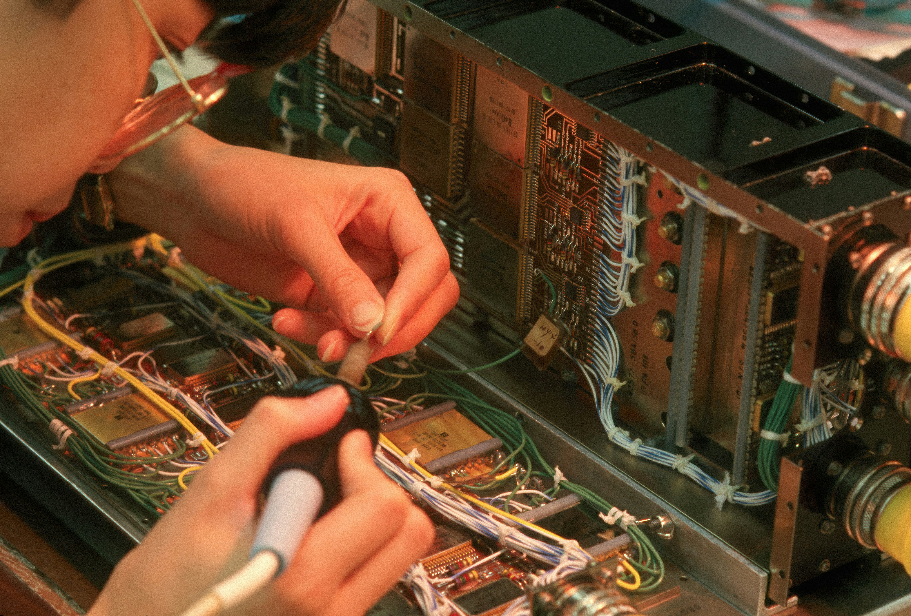
And honestly? Who can blame them. The gap between modern developer tooling and hardware design tooling is embarrassing. I've seen both sides of this. At Apple and Meta I worked with world-class developer tooling — fast iteration loops, strong automation, AI copilots. I built a robotic surgical arm that had to work under rocket launch vibrations through NASA's RockSat program. On the hardware side, the workflow still looks like it did decades ago. Now I'm building Trace, an AI-native PCB design tool. Our team includes engineers from NVIDIA who've designed at the ASIC level. We've seen what world-class dev tooling looks like, and we've seen what the hardware side is stuck with. The gap between those two worlds is insulting.
Software vs Hardware
Software engineers have AI copilots like Cursor and Claude Code writing code alongside them. Instant feedback loops from linters like ESLint and Prettier catching mistakes on every keystroke. Version control on GitHub lol. branch, PR, merge, done. CI/CD on GitHub Actions and CircleCI running tests automatically on every push. Package managers like npm and pip pulling in any dependency with one command. Frameworks like Next.js and Django scaffolding entire apps in minutes. The entire workflow is integrated, fast, and AI-native.
Hardware engineers have Altium charging thousands per year for what is still a manual workflow. KiCad, free but manual everything. OrCAD that takes months just to learn. Version control means renaming files "_final_v2_REAL". Component selection means opening Digi-Key in one tab, LCSC in another, and a PDF datasheet in a third. DRC is a button you click and pray. Routing is done trace by trace, by hand, for hours. Gerber export is a 12-step wizard you google every time. Separate files for every copper layer, silkscreen, solder mask, paste, outline, and drill. Zip them up, upload to JLCPCB or PCBWay, and pray your design rules match their manufacturing constraints. They usually don't. Minimum trace width, annular ring, via diameter, solder mask clearance. Every fab has different specs, and if you violate any of them, you're back in your EDA tool fixing things and re-exporting. Collaboration means emailing a zip file. The UIs have gotten prettier, but the workflow underneath hasn't changed.
To be fair, the premium tools do have semi-automation features that KiCad doesn't. Altium and Allegro offer push-and-shove interactive routing, room replication for multichannel designs, constraint-driven clearance enforcement, and length matching wizards. These are features that save time on specific subtasks. But they're power-user shortcuts, not design automation. The engineer still decides where every component goes, still routes every critical trace, still makes every tradeoff. None of these tools reason about your design. They enforce rules you've already set, but they don't derive those rules from a datasheet or understand the cascading consequences of a design decision. The thinking is still entirely on the engineer.

Why Now
You might ask: if the problem is this obvious, why hasn't anyone solved it? Because until recently, they couldn't. When the first wave of LLMs arrived in 2023, they were impressive at generating text and code - but they were terrible at understanding the kind of problem PCB design actually is. It's not just language. It's multi-domain reasoning: electrical, spatial, thermal, mechanical, and manufacturing constraints all at once, with tradeoffs that cascade across domains. Early models couldn't hold that kind of complexity in context. They'd hallucinate component values, ignore physical constraints, or produce designs that looked plausible but violated basic electrical rules.
That's changing. Recent advances in frontier models (deeper reasoning, longer context, better spatial understanding) have shown that while there's still a long way to go, the possibility is no longer ruled out. Models like GPT-5.4 and Claude Opus 4.6 are scoring higher than humans on SWE benchmarks and reasoning through multi-step constraint problems that would've tripped up earlier models completely. The same kind of reasoning (balancing tradeoffs across conflicting constraints) is exactly what PCB design demands. That doesn't mean you point a language model at an EM problem and hope for the best. The AI handles the reasoning layer: understanding design intent, making tradeoff decisions, reading datasheets and extracting circuits. The physics still runs through real solvers, EM simulation, SPICE, and constraint engines. The breakthrough is combining the two.
The models aren't perfect, but they're good enough to be genuinely useful: reading a 200-page datasheet and extracting the application circuit, understanding that a decoupling cap needs to be within 2mm of the power pin and why, reasoning about how moving one component changes the routing which changes the impedance which changes the stackup. Not just flagging that something's wrong - understanding the design intent behind why it should be a certain way. The gap between "AI can't do this" and "AI can assist with this" is closing faster than anyone expected.
The Research
We're not claiming we've solved this. We haven't. PCB design is one of the hardest problems AI can be pointed at, and there's a long road ahead. But we're doing the research in-house, and the landscape is moving fast. In 2021, Google DeepMind published a paper in Nature showing that reinforcement learning could generate chip floorplans that matched or beat human experts - they've since open-sourced it as AlphaChip. DREAMPlace reframed placement as a neural network training problem and achieved 40x speedups on GPU. TransPlace showed that graph neural networks can learn transferable placement knowledge across unseen circuit designs with 30% less congestion.
ChipDiffusion out of UC Berkeley used diffusion models for zero-shot chip placement, training on synthetic data and generalizing to real circuits. And PCB-Bench, accepted at ICLR 2026, finally gave the field its first real benchmark for LLMs on PCB tasks: 170+ complete projects, 3,700+ annotated instances. Most recently, Cypress (Cornell + NVIDIA, ISPD 2025 Best Paper) became the first to apply VLSI-inspired placement to PCBs with GPU acceleration, achieving up to 492x speedup and 5.9x routability improvement. And Component Centric Placement showed that combining deep RL with simulated annealing on real PCBs produces near human-like results. The field is moving fast, but PCB-specific placement research is still wide open compared to ASIC and VLSI.
PCB is harder. More constraint dimensions, more component types, tighter physical coupling between placement and routing. But the math underneath all of it is the same foundation we're building on. Every placement problem reduces to minimizing wirelength over a graph. Your netlist is a hypergraph - build the graph Laplacian L = D − A (degree matrix minus adjacency matrix), and minimizing total wirelength becomes minimizing xTLx, a quadratic form. The optimal placement coordinates come from solving the sparse linear system Lx = b. This is the foundation of every analytical placer since the 1990s. DREAMPlace builds on it. But it only gives you a continuous relaxation - the "spread everything out evenly" solution. The real constraint satisfaction (DRC, EMC, thermal) lives in the combinatorial space on top.
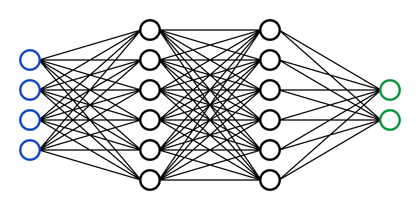
That's where learned heuristics come in. A graph neural network learns the structure of the netlist graph - which components are tightly coupled, which nets are timing-critical, which clusters belong together. Instead of hand-tuning your simulated annealing cooling schedule, the GNN predicts it. Instead of uniform random moves, the GNN proposes moves that respect the graph topology. Our approach at Trace: graph-based learned heuristics paired with simulated annealing. The GNN handles the "what should move where" reasoning. SA handles the search dynamics with a provable convergence guarantee via the Boltzmann acceptance criterion, P(accept) = e−ΔE/kT, from statistical mechanics. Pure SA with hand-tuned parameters gets stuck in local minima on complex boards. Pure GNN placement doesn't handle the constraint diversity of PCB. Together, the network learns constraint-aware move proposals while SA provides the mathematically grounded search framework. We're publishing our early research openly. There are very early signs. The models are starting to reason about constraints in ways that genuinely surprise us. Not perfectly, not every time, but enough to know this isn't a dead end.
Our Approach
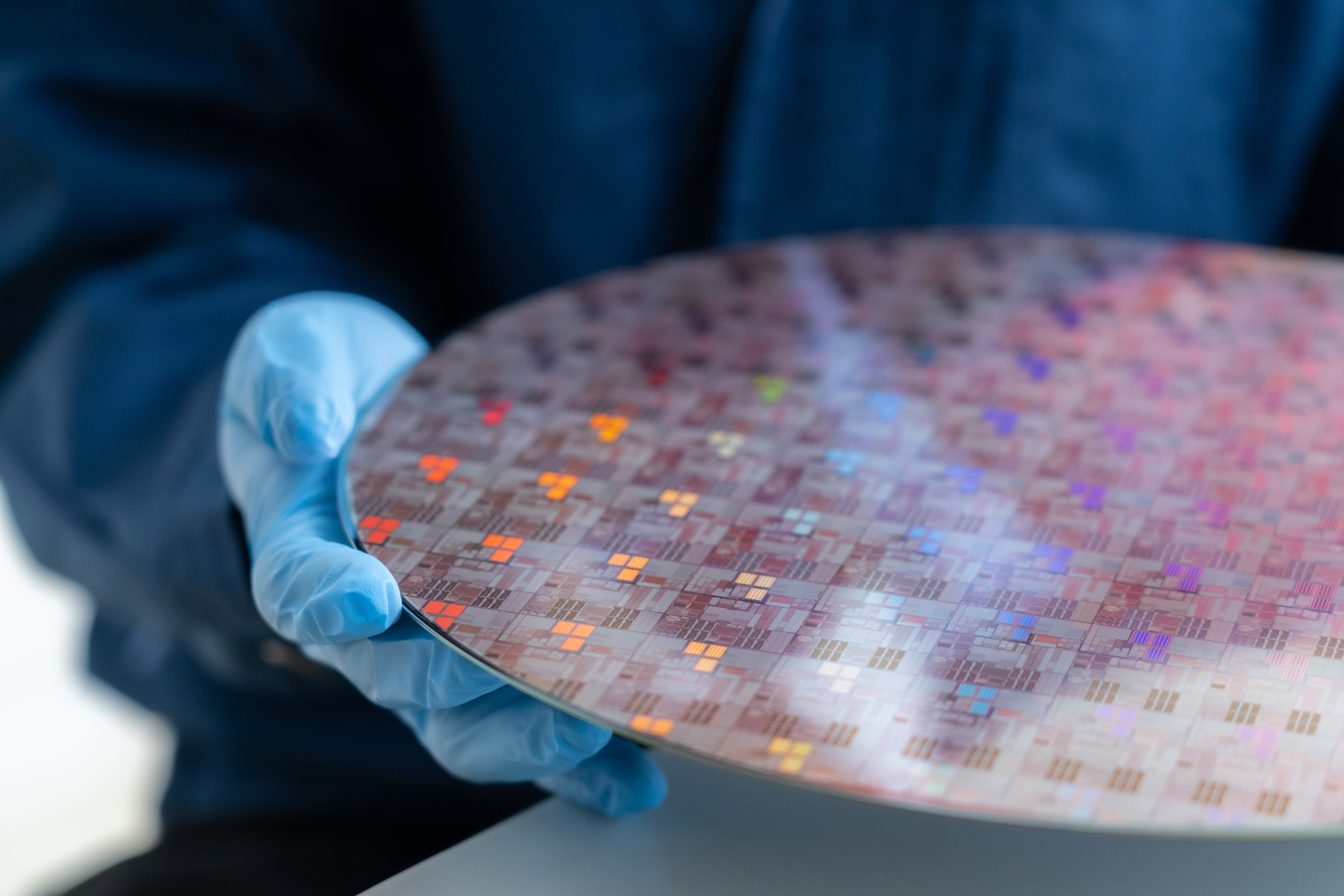
But the research is only half of it. The other breakthrough is how we interface AI with the design itself. Most people's first instinct is to get AI to click through a GUI, or use visual understanding of what's on screen. We went a different direction. We built our own low-level representation of the problem — a proprietary intermediate format that the AI reads and writes directly. The AI reasons about your circuit at the structural level: components, connections, constraints, spatial relationships. Then we convert that into KiCad's native format, reload the editor, and the visual feedback loop serves as the final validation step. The AI doesn't need to "see" your schematic to edit it. It understands the structure underneath. This is the best tool available in its category right now, and honestly it's not even close. And the models are improving by an order of magnitude - every improvement flows directly into Trace. That's the bet, and the trajectory so far says we're right.
This is what gets us excited about building Trace. AI doesn't only speed up the experienced engineer; I like to think of it as two-sided because it also gives the young engineer and the beginner a shot at designing something meaningful. You won't need 15 years of tribal knowledge to place components correctly when the AI understands spacing rules, stackup constraints, and EMC considerations. We're not there yet, but the direction is clear. You won't need to memorize DRC rules when the tool runs them for you in real time.
We're not replacing engineers. We're 10x-ing them. The veteran gets to move faster and focus on the hard problems. The newcomer gets to actually build something instead of spending six weeks just learning the tool.
Beyond PCB
The semiconductor talent crisis is even more severe. The chip industry needs engineers with expertise in VLSI design, embedded systems, and AI chip architecture, and universities can't produce them fast enough. As chip complexity increases with smaller nodes and 3D integration, the hours per tape-out keep going up.
And here's the irony: AI is driving the biggest surge in chip demand in decades. Data centers, edge inference, autonomous vehicles. But we don't have enough engineers to design the chips that AI runs on. The CHIPS Act is pouring $52.7 billion into domestic semiconductor manufacturing, and the fabs are getting built. But a fab without designers is just an expensive building. The bottleneck was never the factories. It's the people.
The Manufacturing Gap
But the talent gap isn't just at the design layer. It extends all the way through manufacturing. Today, the path from finished PCB design to manufactured board is almost entirely outsourced to China. Over 50% of the world's PCBs are manufactured in China, and for good reason: decades of supply chain optimization, cheap labor, and vertically integrated component ecosystems. Most Western engineers don't choose Chinese fabs because they prefer them. They choose them because the tooling funnels them there. Export your Gerbers, upload to JLCPCB or PCBWay, and you're in Shenzhen's pipeline whether you thought about it or not.
This dependency is becoming a strategic liability. In December 2025, the FCC banned all foreign-manufactured drones and critical components - including electronic speed controllers, flight controllers, motors, and radios - from obtaining new FCC authorization for U.S. sale. The CHIPS Act is explicitly about reshoring semiconductor manufacturing. Defense contractors are scrambling to qualify domestic and allied-nation supply chains. But you can't reshore manufacturing if every design tool still optimizes for Chinese fab specs by default. The design tool is the first decision point. It determines which components are selected, which manufacturer constraints are targeted, and which supply chain the entire product flows through.
This is where the real unlock is. Every EDA tool today treats manufacturing as someone else's problem. You design in Altium or KiCad, then manually figure out who can actually build it. You check fab capabilities, cross-reference component availability, negotiate lead times, and pray your design rules align with what JLCPCB can actually produce. That handoff between design and manufacturing is where billions of dollars in inefficiency hide: respins from DFM violations, weeks lost to component substitutions, entire production runs delayed because a single part went end-of-life.
What if the design tool knew the manufacturer? Not as an afterthought, but from the first component placement. Real-time DFM checks against the actual fab you're targeting. Component selection filtered by what's in stock at your preferred distributor. Stackup suggestions that match your manufacturer's standard offerings. One-click ordering with pre-validated design rules. The design tool becomes the control plane for the entire hardware supply chain.
We're already building this. We're partnering with turnkey fabs and assembly houses - the kind that handle PCB fabrication, component sourcing, and board assembly all under one roof. The goal is that when you finish a design in Trace, you don't export Gerbers and go shopping for a manufacturer. You click ship. The tool already knows the fab's capabilities, already validated your design against their DFM rules, already checked that every component is in stock. Fabrication, sourcing, and assembly - all at once, from inside the design environment. (We'll have a major announcement on this soon.)
There's also a labor dimension. Hardware engineering talent is globally distributed, but the tools aren't. A verification engineer in Bangalore or a PCB designer in Taipei has the same technical ability as their counterpart in San Jose, at a fraction of the cost. Companies are already proving this model works in adjacent spaces: partnering with Synopsys and Cadence to run chip verification with distributed teams, using world-class tools with labor arbitrage. It's not outsourcing in the old sense. It's verticalized talent leverage. The bottleneck isn't the engineers. It's that the design tools assume everyone is sitting in the same office, using the same fab, ordering from the same distributor. A tool that's natively connected to regional manufacturers and component suppliers doesn't just help Western companies diversify away from China. It lets any team, anywhere, go from design to manufactured board without the manual supply chain gauntlet.
The world is splitting into competing supply chain blocs. The U.S. and allied nations are reshoring semiconductor fabs. The EU Chips Act, India's semiconductor mission, TSMC expanding into Arizona and Japan: they're all bets on the same thesis. Sovereign hardware capability matters. But sovereignty without design tools is just policy. You need the infrastructure layer that turns engineering talent into manufactured boards, regardless of where the engineer or the fab is located.
The Bet
The best hardware engineers in the world shouldn't have to fight their tools. And the next generation shouldn't have to choose software just because the tooling respects their time. Hardware design shouldn't be held back by outdated tools and decades of unwritten knowledge. The $19 billion EDA market is ready for something new. AI is the catalyst, and every design that runs through the system makes the next one better. Trace is our attempt to rebuild the infrastructure for how hardware gets designed: from the first schematic to the manufactured board, across any supply chain, for any engineer, anywhere - buildwithtrace.com.
— Ayomide Adekoya
Co-Founder & CEO, Trace